Thursday, January 31, 2008

PROCEDURE ON DVD RECORDING


1. DVD recorders in the closet should be on already and should not be turned off. If the power happens to be off, press the power button to turn the machine on, but there is a time lag of 5-10 minutes before the machine is ready to record.

2. Press the [OPEN/CLOSE] button to open the DVD drive bay and insert the DVD-Ram disk. Do not use DVD-R, DVD-RW, or CD-RW disks.

3. Press the [OPEN/CLOSE] button again to close the drive.

4. Press the [CHANNEL UP / DOWN] button to set the recorder to your office channel.

5. Press the [RECORD] button to begin recording.

6. Flip the camera switch in your office to [ON] after the client gives their consent to be recorded.

7. When recording is finished, press the [STOP] button.

8. Press the [OPEN/ CLOSE] button to open the drive door and remove the disk from the drive. Press the [OPEN/ CLOSE] button again to close the drive

Thursday, January 24, 2008

Socket A / socket 462


Socket A (also known as Socket 462) is the CPU socket used for AMD processors ranging from the Athlon Thunderbird to the Athlon XP/MP 3200+, and AMD budget processors including the Duron and Sempron. Socket A also supports the recent AMD Geode NX embedded processors (derived from the Mobile Athlon XP). The socket is a zero insertion force pin grid array type with 453 pins (nine pins are blocked in the socket to prevent accidental insertion of Socket 370 CPUs, hence the number 462). The front side bus frequencies supported for the AMD Athlon XP and Sempron are 133 MHz, 166 MHz, and 200 MHz.
AMD recommends that the mass of a Socket A CPU cooler not exceed 300
grams (10.6 ounces). Heavier coolers may result in damage to the die when the system is not properly handled.
Socket A has been discontinued in favor of
Socket 754, Socket 939, and recently Socket AM2, except for its use with Geode NX processors. However, microprocessors and motherboards from many vendors are still available

Socket 563


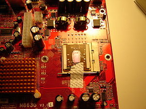
Socket 563 is a microPGA CPU socket used exclusively for low-power (16 W and 25 W TDP) Athlon XP-M processors (Models 8 & 10).
This socket can usually be found on
laptops and requires a low-power mobile part in a special 563-pin µPGA package which is different from the Socket A (453 pin) package used for other Athlon processors.
There exists
desktop computer motherboards equipped with socket 563. PCChips is known to have marketed such a board, the M863G Ver3 (actually made by ECS), bundled with a socket 563 processor and a heatsink.

Wednesday, January 23, 2008

Socket 603


Socket 603
is a motherboard socket for Intel's Xeon processor.

Socket 603 was designed by Intel as a Zero Insertion Force socket intended for workstations and server platforms. It contains 603 contacts arrayed about the center of the socket, each contact has a 1.96mm pitch with regular pin array, to mate with a 603-pin processor package. Intel's design notes distinguish Socket 603 from Socket 604 as low cost, low risk, robust, high volume manufacturable, and multi-sourceable.[1]

All Socket 603 processors utilize a bus speed of 400 MHz and were manufactured in either a 180 nm process, or 130 nm process. Socket 603 processors can be inserted into Socket 604 designed motherboards, but Socket 604 processors cannot be inserted into Socket 603 designed motherboards due to one additional pin being present. Currently, Socket 603 processors range from 1.4 GHz, to 3 GHz.

Socket 775


On June 22nd Intel launched their socket-775 platform which meant the introduction of a new socket for Pentium 4 processors and two new chipsets. Initially we were skeptic about the new socket-775, many of the motherboard manufacturers we talked to described it as fragile and they were expecting many product returns due to customers damaging the socket. In the past few months we’ve worked with quite a few socket-775 motherboards and we can honestly say that socket-775 isn’t as fragile as we thought. If you insert and remove the processor as intended you won’t damage the socket, nor will it cease to function after a few insertions.

Socket 479


Socket 479 is the CPU socket for the Intel Pentium M, a mobile processor, normally used in laptops, as well as Tualatin-M Pentium III processors. The official naming by Intel is mFCPGA and mPGA479M. Despite the 479 in the name the Pentium M Processors for this socket use only 478 Pins.

It uses a different electrical pin-arrangement from socket 478, making it impossible to use a Pentium M in a normal 478 board, but yet the Pentium M fits mechanical in a Socket 478. For this reason Asus makes a drop-in board (CT-479) which lets you use socket 479 processors in selected Asus boards. Currently, the only chipsets for the Pentium M are the Intel 855GM/GME, Intel 915GM and Intel 6300ESB. While the Intel 855GME chipset supports all Pentium M CPU's, the Intel 855GM chipset does not support the 90nm 2MB L2 cache (Dothan core) ones.

Recently, Intel has released a new socket 479 with a revised pinout for its Core processor, called Socket M. This socket has the placement of one pin changed from the original Socket 479 in order to make the different processors incompatible in the incorrect socket. Socket M supports a 667 MT/s front side bus with the Intel 945GM chipset.

Socket 423


Socket 423
was a CPU socket used for the first Pentium 4 processors, based on the Willamette core. The socket was short-lived, as it became apparent that its electrical design proved inadequate for raising clock speed beyond 2.0 GHz. Intel produced chips using this socket for less than a year, from November 2000 to August 2001. It was replaced by Socket 478.

The "PowerLeap PL-P4/N" is a device developed in the form of a socket adapter allowing the use of socket 478 processors on the socket 423.

Along with the socket these CPUs use (and therefore the motherboards), there is another short lived and odd piece of hardware: the RAM. The type of RAM used on some of these motherboards is RDRAM. This type of RAM is now very expensive, ranging from $US54 for 128MB to $US214 for 512MB. These sticks of RAM also must be installed in pairs, similar to SIMMs in older classic Pentium systems.

Socket 478


In computing, Socket 478 is a type of CPU socket used for Intel's Pentium 4 and Celeron series CPUs. Socket 478 was phased out with the launch of LGA775.

Socket 478 has been used for all of the Northwood Pentium 4s and Celerons, the first Prescott Pentium 4s, and some Willamette Celerons and Pentium 4s. Socket 478 also supports newer Prescott Celeron Ds, and early Pentium 4 Extreme Edition processors with 2MB of L3 cache and some Core Duos. The socket was launched with the Northwood core to compete with AMD's 462-pin Socket A and their Athlon XP processors. Socket 478, which accommodates high and low-end processors, was also the replacement for Socket 423, a Willamette processor socket which remained in the market for only a short time.

Motherboards that use this socket support DDR, RDRAM, and in some cases SDRAM. However, the majority of boards are DDR based. Initial motherboards only supported RDRAM, however RDRAM is quite expensive, compared to DDR and SDRAM, and consumers demanded an alternative, thus DDR and SDRAM boards were made. Later revisions to chipsets that support Socket 478 added higher FSB speeds, higher DDR speeds, and support for dual channel DDR.

Like the previous Socket 423, Socket 478 is based on Intel's Quad Data Rate technology, with data transferring at four times the clock rate of its Front Side Bus. As such, the 400 MT/s bus was based on a 100 MHz clock signal, but was still able to provide 3.2GB/s of data to the chipset. At its release, no SDRAM product was capable of supporting so high a data rate, so Intel pushed forward RDRAM technology, with two channels of PC800 providing synchronous data capability. Poor consumer acceptance of expensive RDRAM lead Intel to release low-performance PC133-supporting chipsets, and finally DDR chipsets.

Socket 940


Socket 940
is a 940-pin socket for 64-bit AMD server processors. The socket is entirely covered with leads, except for four key pins used to align the processor. AMD Opterons and the older AMD Athlon 64 FX (FX-51) use Socket 940. Being an intended server platform, processors using this socket only accept registered memory, because, in servers, memory errors are less acceptable and cause more damage.

The more common use of Socket 940 is in the Server market. Dual Socket 940 boards use the 200-series Opterons. Four(Common) or Eight(Rare) socketed boards use the 800-series Opterons. The Socket 940 platform is designed for raw power and professional accuracy, not bleeding-edge gaming performance.

There is a new 940-pin socket called AM2. Though the current Socket 940 and the AM2 both share the same number of pins, they are not pin-compatible. That is, a Socket 940 processor will not fit in a AM2 socket. The same is true in reverse; a Socket AM2 processor will not fit in Socket 940. The reason for this is because all 64-bit AMD processors, unlike all current Intel processors, include the memory management functionality not as a discrete chip on the motherboard, but rather on the CPU die itself.

Socket 939


Socket 939
is a CPU socket released by AMD in June 2004 to supersede the previous Socket 754 for Athlon 64 processors. Socket 939 has been succeeded by Socket AM2, although Socket 939 is still popular. It is the second socket designed for AMD's AMD64 range of processors.

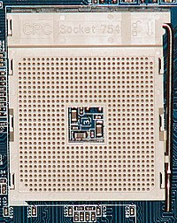
Socket 754


Socket 754
is a CPU socket originally developed by AMD to succeed its Athlon XP platform (Socket 462, also referred to as Socket A). Socket 754 was the first socket developed by AMD to support their new consumer version of the 64 bit microprocessor family known as AMD64.

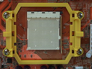
Socket AM2


The Socket AM2, renamed from Socket M2 (to prevent using the same name as Cyrix MII processors), is a CPU socket designed by AMD for desktop processors, including the performance, mainstream and value segments. It was released on May 23, 2006, as a replacement for Socket 939 & Socket 754.

Socket S1

Socket S1 is the CPU socket type used by AMD for their Turion 64, Athlon 64 Mobile and later Sempron processors, which debuted with the dual core Turion 64 X2 CPUs on May 17, 2006. Socket S1 has 638 pins, and replaces the existing Socket 754 for laptops. It has been expected that desktop motherboards will appear using Socket S1, much as boards using the Pentium M's Socket 479 are on the market.

Socket S1 includes support for dual-channel DDR2 SDRAM, dual-core mobile CPUs, and virtualization technology, to compete with the mobile Intel Core 2 processor series.

Socket S1 is a part of AMD's next generation of CPU sockets, along with Socket F (servers) and Socket AM2 (desktop).

Socket 370 - PGA (Pin Grid Array)


Socket 37 is a common format of CPU socket first used by Intel for Pentium III and Celeron processors to replace the older Slot 1 CPU interface on personal computers. The "370" refers to the number of holes in the socket for CPU pins. Modern Socket 370 fittings are usually found on Mini-ITX motherboards and embedded systems.
Socket 370 was originally used for the Intel
Celeron, but later became the socket/platform for the Coppermine and Tualatin Pentium III processors, as well as the Via-Cyrix Cyrix III, later renamed the VIA C3. Some motherboards that used Socket 370 support Intel processors in dual CPU configurations. Others allowed the use of a Socket 370 or Slot 1 CPU, although not at the same time.
The weight of a Socket 370 CPU cooler should not exceed 180 gram. Heavier coolers may result in damage to the die when the system is not properly handled.
This platform is not wholly obsolete, but its use is today limited to the above specialty applications, having been superseded by Socket
423/478/775 (for Pentium 4 and Core 2 processors). Via is at present still producing Socket 370 processors but committed to migrating their processor line to ball grid array packages

Thursday, January 17, 2008

FORM FACTORS - MOTHERBOARD

AT & Baby AT
Prior to 1997, IBM computers used large motherboards. After that, however, the size of the motherboard was reduced and boards using the AT (Advanced Technology) form factor was released. The AT form factor is found in older computers (386 class or earlier). Some of the problems with this form factor mainly arose from the physical size of the board, which is 12" wide, often causing the board to overlap with space required for the drive bays.

Following the AT form factor, the Baby AT form factor was introduced. With the Baby AT form factor the width of the motherboard was decreased from 12" to 8.5", limiting problems associated with overlapping on the drive bays' turf. Baby AT became popular and was designed for peripheral devices — such as the keyboard, mouse, and video — to be contained on circuit boards that were connected by way of expansion slots on the motherboard.

Baby AT was not without problems however. Computer memory itself advanced, and the Baby AT form factor had memory sockets at the front of the motherboard. As processors became larger, the Baby AT form factor did not allow for space to use a combination of processor, heatsink, and fan. The ATX form factor was then designed to overcome these issues.
Key Terms To Understanding Motherboard Form Factors
motherboard
The main circuit board of a microcomputer.

form factor
The physical size and shape of a device. It is often used to describe the size of circuit boards.

AT
Short for advanced technology, the AT is an IBM PC model introduced in 1984.

ATX
The modern-day shape and layout of PC motherboards.

BTX
The BTX specification provides new tools and design space for developers to lay out desktop systems, whether designing small, compact systems or very large, expandable systems.

Baby AT
The form factor used by most PC motherboards prior to 1998.


ATX
With the need for a more integrated form factor which defined standard locations for the keyboard, mouse, I/O, and video connectors, in the mid 1990's the ATX form factor was introduced. The ATX form factor brought about many chances in the computer. Since the expansion slots were put onto separate riser cards that plugged into the motherboard, the overall size of the computer and its case was reduced. The ATX form factor specified changes to the motherboard, along with the case and power supply. Some of the design specification improvements of the ATX form factor included a single 20-pin connector for the power supply, a power supply to blow air into the case instead of out for better air flow, less overlap between the motherboard and drive bays, and integrated I/O Port connectors soldered directly onto the motherboard. The ATX form factor was an overall better design for upgrading.

micro-ATX
MicroATX followed the ATX form factor and offered the same benefits but improved the overall system design costs through a reduction in the physical size of the motherboard. This was done by reducing the number of I/O slots supported on the board. The microATX form factor also provided more I/O space at the rear and reduced emissions from using integrated I/O connectors.

LPX
White ATX is the most well-known and used form factor, there is also a non-standard proprietary form factor which falls under the name of LPX, and Mini-LPX. The LPX form factor is found in low-profile cases (desktop model as opposed to a tower or mini-tower) with a riser card arrangement for expansion cards where expansion boards run parallel to the motherboard. While this allows for smaller cases it also limits the number of expansion slots available. Most LPX motherboards have sound and video integrated onto the motherboard. While this can make for a low-cost and space saving product they are generally difficult to repair due to a lack of space and overall non-standardization. The LPX form factor is not suited to upgrading and offer poor cooling.

NLX
Boards based on the NLX form factor hit the market in the late 1990's. This "updated LPX" form factor offered support for larger memory modules, tower cases, AGP video support and reduced cable length. In addition, motherboards are easier to remove. The NLX form factor, unlike LPX is an actual standard which means there is more component options for upgrading and repair.

Many systems that were formerly designed to fit the LPX form factor are moving over to NLX. The NLX form factor is well-suited to mass-market retail PCs.

BTX
The BTX, or Balanced Technology Extended form factor, unlike its predecessors is not an evolution of a previous form factor but a total break away from the popular and dominating ATX form factor. BTX was developed to take advantage of technologies such as Serial ATA, USB 2.0, and PCI Express. Changes to the layout with the BTX form factor include better component placement for back panel I/O controllers and it is smaller than microATX systems. The BTX form factor provides the industry push to tower size systems with an increased number of system slots.

One of the most talked about features of the BTX form factor is that it uses in-line airflow. In the BTX form factor the memory slots and expansion slots have switched places, allowing the main components (processor, chipset, and graphics controller) to use the same airflow which reduces the number of fans needed in the system; thereby reducing noise. To assist in noise reduction BTX system level acoustics have been improved by a reduced air turbulence within the in-line airflow system.

Initially there will be three motherboards offered in BTX form factor. The first, picoBTX will offer four mounting holes and one expansion slot, while microBTX will hold seven mounting holes and four expansion slots, and lastly, regularBTX will offer 10 mounting holes and seven expansion slots. The new BTX form factor design is incompatible with ATX, with the exception of being able to use an ATX power supply with BTX boards.

Today the industry accepts the ATX form factor as the standard, however legacy AT systems are still widely in use. Since the BTX form factor design is incompatible with ATX, only time will tell if it will overtake ATX as the industry standard.